Key Takeaways
- OpenAI and Broadcom claim Jalapeño delivers 1.5x to 1.9x higher peak throughput per watt than Nvidia’s GB200 and GB300 systems.
- The chip draws 700W against roughly 1,200W for GB200 and 1,400W for GB300, so the efficiency gain comes largely from running cooler and slower rather than faster.
- OpenAI reports 1.7x to 3.6x lower end-to-end latency and 2.1x to 4.1x lower minimum time between tokens compared with the same Blackwell parts.
- Jalapeño carries 216 GB of HBM4 with up to 15.4 TB/s of bandwidth, and peaks at 3.4 MXFP8 PFLOPS or 13.4 MXFP4 PFLOPS.
- It is an inference-only accelerator. Blackwell trains and serves models; Jalapeño only serves them.
- A full pod links 2,048 chips across 16 racks for 27 EFLOPS at MXFP4, 432 TB of HBM4 and 32 PB/s of aggregate memory bandwidth.
- Design to tape-out took nine months, unusually fast for a reticle-sized ASIC, with Broadcom handling silicon and networking and Celestica the board and rack integration.
- Every published comparison is vendor-supplied. No independent benchmark results existed at the time of the Hot Chips 2026 disclosure, and OpenAI has promised a detailed performance report later.
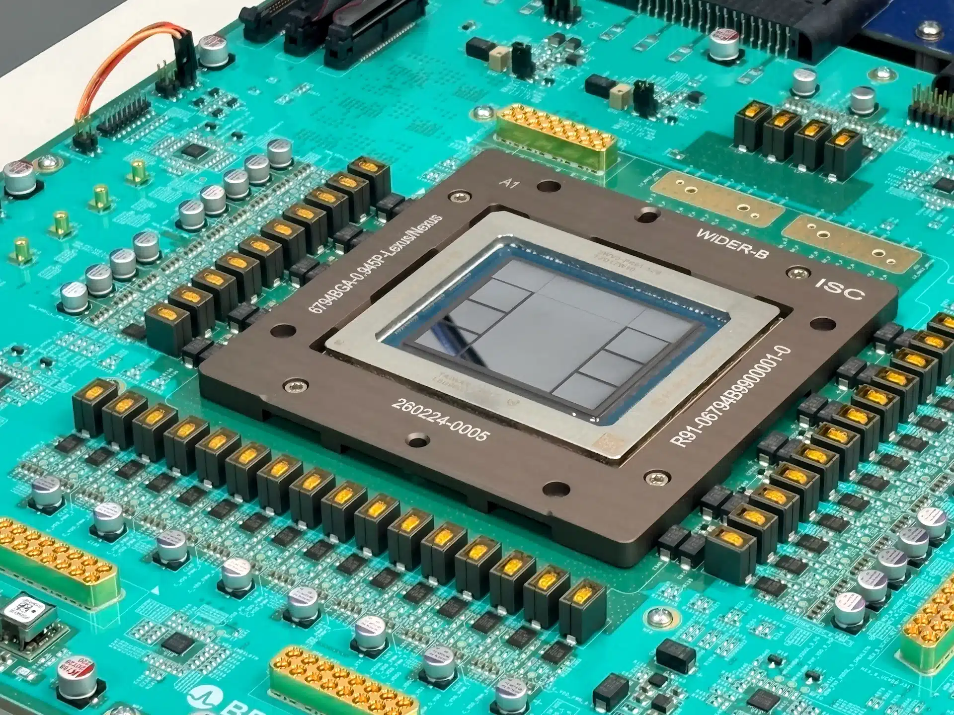
OpenAI Jalapeño chip. Image credit: OpenAI
On the numbers OpenAI has published, Jalapeño beats Nvidia Blackwell on efficiency and latency while losing on flexibility. The chip produces between 1.5 and 1.9 times more peak throughput per watt than GB200 and GB300 systems, answers requests with 1.7 to 3.6 times lower end-to-end latency, and cuts the minimum gap between generated tokens by 2.1 to 4.1 times. It does all of this while drawing 700W, roughly half the power of a GB300 accelerator.
Those advantages come from a narrow design brief. Jalapeño was built from the ground up for large language model inference and does nothing else, whereas Blackwell is a general accelerator that trains frontier models, serves them, and runs scientific and graphics workloads besides. Comparing the two is therefore a comparison between a specialist and a generalist, and the specialist wins on its own ground by a margin that is large but not unexpected.
What OpenAI and Broadcom Actually Built
Announced on 24 June 2026, Jalapeño is OpenAI’s first custom silicon, produced with Broadcom as the implementation and networking partner. It is a reticle-sized ASIC — physically about as large as a chip can be made — and it went from design start to tape-out in nine months, a schedule that would be aggressive for a far simpler part.
The architecture is spatial rather than monolithic. The die is divided into 64 memory and core slices arranged in a NUMA-style layout, with a high-bandwidth, low-latency collective network connecting cores directly. That arrangement targets the specific bottleneck in transformer inference: moving activations and key-value cache data around, not raw multiply-accumulate capacity. OpenAI’s stated goal is realised utilisation much closer to theoretical peak, which is where general-purpose accelerators typically leave performance on the table.
Memory is the headline specification. Jalapeño carries 216 GB of HBM4 with up to 15.4 TB/s of bandwidth — the first generation of HBM4 to appear in a shipping inference part, and a capacity that lets larger models and longer contexts stay resident without spilling.
Jalapeño and Blackwell Side by Side
| Attribute | OpenAI Jalapeño | Nvidia GB200 | Nvidia GB300 |
|---|---|---|---|
| Purpose | LLM inference only | Training and inference | Training and inference |
| Power per accelerator | 700W | ~1,200W | ~1,400W |
| Memory | 216 GB HBM4 | 192 GB HBM3E per GPU | 288 GB HBM3E per GPU |
| Memory bandwidth | Up to 15.4 TB/s | 8 TB/s class | 8 TB/s class |
| Peak low-precision throughput | 13.4 PFLOPS MXFP4 / 3.4 PFLOPS MXFP8 | FP4-class rack throughput | FP4-class rack throughput |
| Clock | 1.70 GHz, rising to 1.80 GHz | Not disclosed comparably | Not disclosed comparably |
| Scale-up domain | 128 accelerators per rack over Ethernet at 600 GB/s | 72 GPUs per NVL72 rack over NVLink | 72 GPUs per NVL72 rack over NVLink |
| Availability | Initial deployment from late 2026 | Shipping since 2025 | Shipping |
Where the Efficiency Advantage Comes From
Three design choices explain most of the gap. The first is precision. Jalapeño’s headline figures are quoted at MXFP4 and MXFP8, microscaling formats that suit inference well because serving a trained model tolerates lower numerical precision than training one. Blackwell supports low precision too, but carries the silicon area for higher-precision training work that an inference chip can simply omit.
The second is power envelope. At 700W, Jalapeño sits well down the voltage-frequency curve where efficiency is best. Blackwell parts push toward the top of that curve to maximise absolute throughput, which is the right call for training runs measured in weeks and the wrong one for per-token efficiency. Roughly half the claimed per-watt advantage is a consequence of that choice rather than of architectural novelty.
The third is data movement. By reducing the distance activations travel and building the collective network into the die, the design attacks the memory-bound nature of token generation directly. That is also why the latency figures — 1.7x to 3.6x lower end to end — are larger than the throughput figures. Latency is where a purpose-built inference part shows its work, and it matters commercially, because tokens are the unit that generative AI is billed in.
What Blackwell Still Does That Jalapeño Cannot
Blackwell trains models. Jalapeño does not, and OpenAI has not suggested it will. Any lab deploying Jalapeño at scale still buys Nvidia hardware for pre-training and post-training, which means the chip reduces Nvidia purchases rather than replacing them.
Nvidia also brings the software estate. CUDA, cuDNN, TensorRT-LLM, NCCL and two decades of accumulated tooling run on every Blackwell part the day it arrives. A custom ASIC runs the stack its owner writes for it. For OpenAI, which controls its own models and serving infrastructure end to end, that is a manageable cost. For anyone else it would be prohibitive, which is precisely why Jalapeño is not a merchant product.
And Nvidia has not stood still. Blackwell Ultra shipped through 2026, and the Vera Rubin platform entered production in August 2026, expected to account for around 20% of Nvidia’s third-quarter data centre revenue. The relevant comparison a year from now will be Jalapeño against Rubin, not against the parts benchmarked at Hot Chips. Readers can see where those generations sit in the Blackwell Ultra GB300 and Vera Rubin roadmap.
How the Systems Scale
Rack-level design differs sharply. Nvidia builds NVL72 racks around 72 GPUs joined by NVLink, a proprietary high-bandwidth fabric. Jalapeño puts 128 accelerators in a rack connected over Ethernet at 600 GB/s, then links 16 racks into a pod of 2,048 chips at 200 GB/s per processor. The pod totals 27 EFLOPS at MXFP4, 432 TB of HBM4 and 32 PB/s of aggregate memory bandwidth.
Choosing Ethernet over a proprietary fabric is a deliberate trade — lower peak link bandwidth in exchange for commodity switching, easier sourcing and no vendor lock at the network layer. Broadcom’s networking business is the obvious beneficiary, and it is a large part of why OpenAI picked that partner. The same argument shapes how Blackwell servers are configured at the other end of the design space.
How Much of This Can Be Verified
Not much, yet. Every performance ratio published so far comes from OpenAI and Broadcom, measured on workloads they selected. There is no MLPerf submission, no third-party latency testing, and no disclosure of the process node or die size. The chip has run real work — engineering samples executed GPT-5.3-Codex-Spark at production frequency and specification — but running a workload is not the same as an audited comparison.
OpenAI has said a detailed technical report on performance will follow. Until it does, the honest reading is that Jalapeño appears to be a strong inference part with a credible efficiency advantage on the workloads it was designed for, and that the size of that advantage against a fairly configured Blackwell system is unproven.
What It Means for the Custom Silicon Trend
Jalapeño lands in a pattern that now includes Google’s TPU line, Amazon’s Trainium and Inferentia, Meta’s MTIA and Microsoft’s Maia. Every lab large enough to fill a fab reservation is building a part tuned to its own models, because inference is where compute cost turns into gross margin. The economics are simple: if you serve a fixed set of models at enormous volume, a chip that does only that will beat a chip that does everything.
What it does not do is dislodge Nvidia. OpenAI still needs training capacity, still buys Nvidia systems, and has committed to gigawatt-scale deployments that no single supplier can fill. The chip reduces dependence at the margin and gives OpenAI a credible negotiating position, in the same way that Google’s TPU programme and Alphabet’s Frozen v2 chip reduced Alphabet’s. That is a smaller claim than the benchmark ratios suggest, and a more durable one — the logical next step for a company already building out its own cloud.
If you are interested in this topic, we suggest you check our articles:
- NVIDIA Blackwell Server: Specs, Power and Capabilities
- Nvidia’s Blackwell Ultra GB300 and Vera Rubin
- What Is a Tensor Processing Unit (TPU)? A 2026 Guide
- How Alphabet’s Frozen v2 Chip Will Power Gemini Models
- OpenAI’s Infrastructure Push: Becoming Its Own Cloud Provider
Sources: OpenAI, Broadcom, Tom’s Hardware (Hot Chips 2026), Tom’s Hardware (launch), CNBC
Written by Alius Noreika