Key Takeaways
- A Tensor Processing Unit is an application-specific integrated circuit built by Google to accelerate the matrix mathematics at the core of neural networks.
- Its defining component is a systolic array: a grid of multiply-accumulate units that pass data hand to hand, avoiding the repeated memory trips that dominate energy use on general-purpose chips.
- Google built the first TPU in about 15 months after calculating that three minutes of daily voice search per Android user would have required doubling its entire datacentre capacity.
- TPU v1 powered AlphaGo’s 2016 win over Lee Sedol and delivered 15–30x the speed and 30–80x the power efficiency of contemporaneous general-purpose hardware.
- Ironwood (TPU v7, documented as TPU7x) reached general availability on 22 April 2026 with 192 GB of HBM per chip, about 7.37 TB/s of bandwidth, and 4,614 FP8 teraFLOPS.
- A full Ironwood pod links 9,216 chips sharing roughly 1.77 petabytes of memory over a 3D torus interconnect.
- Google previewed an eighth generation on the same day, splitting the line into TPU 8t for training and TPU 8i for inference, both on TSMC’s 2nm process.
- Anthropic is the anchor external customer, committed to up to one million TPU chips and more than a gigawatt of capacity in 2026, rising to 3.5 gigawatts in 2027.
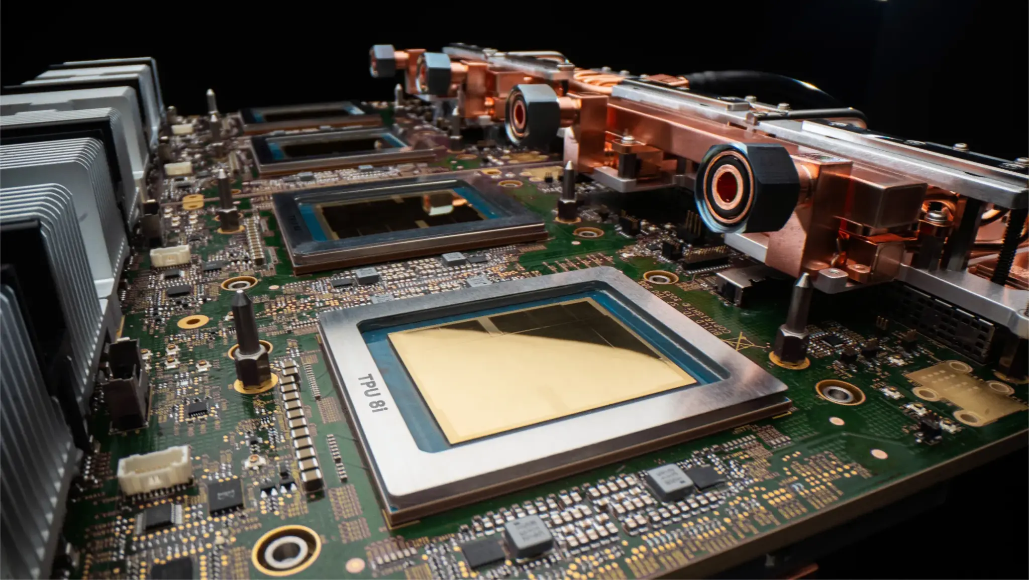
A TPU. Image credit: Google
A Tensor Processing Unit (TPU) is a custom silicon chip designed by Google specifically to run machine learning workloads. It is an application-specific integrated circuit — hardware built for one job rather than adapted to many — and that job is multiplying and adding very large matrices, which is what a neural network spends nearly all of its time doing.
The design choice that separates a TPU from a CPU or a GPU is the systolic array. Instead of fetching operands from memory, computing, and writing results back for every operation, a TPU streams data through a fixed grid of arithmetic units that hand partial results to their neighbours. Memory movement typically consumes 10 to 100 times more energy than the arithmetic itself, so eliminating most of those round trips is where the efficiency comes from.
Why Google Built Its Own Chip
In 2013, Google engineers ran a calculation that changed the company’s hardware strategy: if every Android user spoke to voice search for three minutes a day, Google would need to double its datacentre footprint to serve the demand. Buying more general-purpose servers was not going to work.
The response was TPU v1, developed in roughly 15 months with a single narrow goal — accelerate neural network inference, not training. It went into production in 2015 and became public knowledge in 2016, the same year it powered AlphaGo’s match against Lee Sedol. Google reported gains of 15 to 30 times in speed and 30 to 80 times in performance per watt against the CPUs and GPUs of the day, which established that a purpose-built accelerator could outrun general-purpose silicon by an order of magnitude on a narrow workload.
Inside a TPU: How the Systolic Array Works
Each TPU chip contains one or more TensorCores. A TensorCore holds one or more matrix-multiply units (MXUs), a vector unit for operations like activations and softmax, and a scalar unit that handles control flow and memory addressing.
The MXU is the engine. Through TPU v5p it was a 128×128 systolic array — 16,384 multiply-accumulators working in lockstep. Starting with Trillium (v6e) and continuing into TPU7x, that expanded to 256×256, quadrupling operations per cycle. Each MXU performs 16,000 multiply-accumulate operations per clock cycle. Multiplications take bfloat16 inputs while accumulation happens in FP32, which preserves numerical stability without paying full precision cost on the multiply.
The bit-width trick
Multiplier area on silicon scales with the square of bit width. An 8-bit multiplier occupies roughly 64 units of area; a 32-bit multiplier needs about 576. That relationship is why TPUs can pack so much more arithmetic into a given die than chips built for scientific precision. TPU v1 used 8-bit integers for inference, cutting memory requirements fourfold — a 91 MB model quantises to about 23 MB.
Feeding the array
Compute is only useful if data arrives fast enough. TPU v1 used DDR3 memory delivering 34 GB/s. Ironwood provides roughly 7.37 TB/s of high-bandwidth memory, a 217-fold improvement achieved by stacking DRAM dies vertically with thousands of connections between them. Ironwood also exposes vector memory (VMEM), a smaller on-chip SRAM scratchpad with much higher bandwidth to the MXU than HBM, used by custom kernels.
TPU Generations at a Glance
| Generation | MXU | HBM per chip | Pod scale and topology | Notes |
|---|---|---|---|---|
| TPU v1 (2015) | 256×256 | DDR3, 34 GB/s | Single-chip | Inference only; 65,536 8-bit ops per cycle |
| TPU v2–v3 | 128×128 | — | 2D torus | v3 carried two systolic arrays per processor |
| TPU v5e | 128×128 | 16 GB | 256 chips, 2D torus | Cost-efficient tier |
| TPU v5p | 128×128 | — | 4,096 chips, 3D torus | Performance tier for training |
| TPU v6e (Trillium) | 256×256 | 32 GB, ~1,600 GB/s | 256 chips, 2D torus | 918 bf16 TFLOPs; 4.7x v5e compute; 67% more energy efficient |
| TPU v7 (Ironwood / TPU7x) | 256×256 | 192 GB, ~7.37 TB/s | 9,216 chips, 3D torus | 4,614 FP8 TFLOPS; two chiplets per chip; GA 22 April 2026 |
| TPU 8i (preview) | — | 288 GB, 8.6 TB/s | — | 10.1 FP4 petaflops; 384 MB on-chip SRAM; inference-tuned |
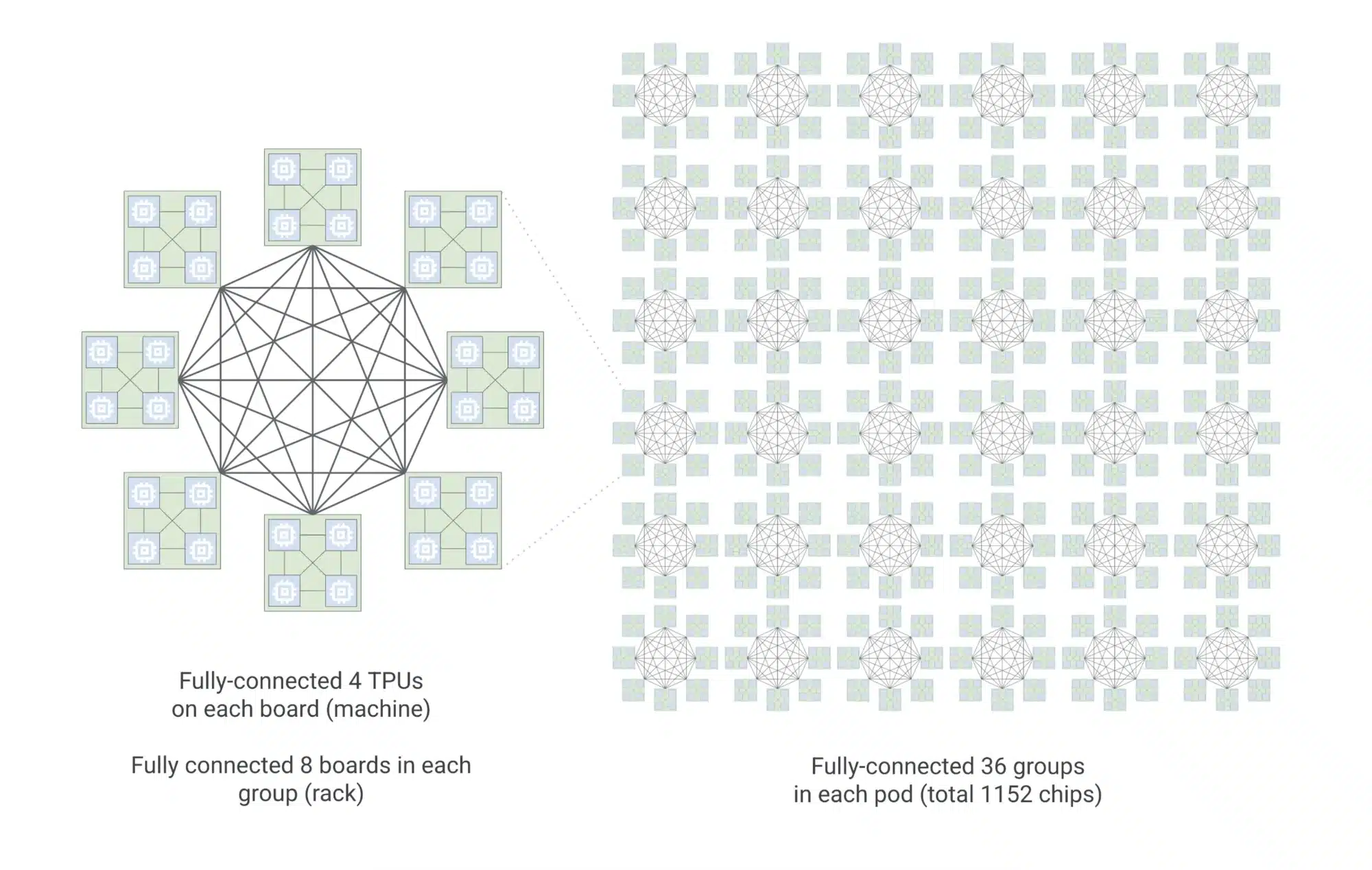
TPU 8i hierarchical Boardfly topology building up from a building block of four fully connected chips into a fully connected group of eight boards, with 36 of such groups fully connected into a TPU 8i pod. Image credit: Google
Ironwood: The Inference Generation
Google made Ironwood generally available at Cloud Next on 22 April 2026, positioning it as its first TPU built for the age of inference rather than training. The architecture departs from earlier designs in a specific way: each Ironwood chip is composed of two distinct chiplets, each a self-contained unit with one TensorCore, two SparseCores, and 96 GB of HBM, connected by a die-to-die interface roughly six times faster than a single inter-chip interconnect link. That replaces the unified memory space of the previous MegaCore approach, and the programming model resembles pre-v4 generations such as v3.
SparseCores matter more than their obscurity suggests. They accelerate the embedding operations that drive ranking and recommendation systems, and they handle the sparse computation patterns typical of mixture-of-experts models — which describes most current frontier architectures.
Google reports Ironwood at roughly ten times the peak performance of v5p and four times the per-chip performance of Trillium. A full pod reaches 9,216 chips sharing about 1.77 petabytes of memory.
The pricing gap
Three months after general availability, Google had still published no on-demand rate for Ironwood, while Trillium and older generations carry public prices. The only figure in circulation is a SemiAnalysis estimate of roughly $1.60 per chip-hour for Anthropic’s negotiated capacity — a contract rate, not a list price. HSBC separately estimated rental economics at $1.50 to $2.00 per hour. Without a published rate card, smaller teams cannot model inference unit costs or compare Ironwood against Nvidia hardware that does list prices, which pushes them toward accelerators they can quote.
TPU vs GPU: Where Each One Wins
| Consideration | TPU | GPU |
|---|---|---|
| Best-fit workloads | Large transformer and CNN training and serving, batch inference | Mixed workloads, irregular compute patterns, rapid prototyping |
| Batch size | Large batches, where the array stays saturated | Small batches and bursty user-facing traffic |
| Software | JAX/XLA, PyTorch/XLA, TensorFlow | PyTorch-native with the widest library ecosystem |
| Availability | Primarily through Google Cloud; rack-level systems now sold via Broadcom | Purchasable and rentable across every major cloud and neocloud |
| Energy profile | Strong performance per watt on dense matrix work | Higher flexibility per watt across varied kernels |
The honest framing is that GPUs did not lose. Nvidia exposed a programming model and developer experience that let GPUs behave much like a TPU for these workloads, which is why they still dominate. TPUs win on specific shapes of problem — and in an era where electricity has become the binding constraint on AI, performance per watt is not a footnote. At 100,000 chips or more, a two-to-three-fold power difference reaches national-scale consumption figures. For the other side of the hardware picture, our overview of what a Blackwell server actually contains covers the rack-scale GPU approach in equivalent detail.
Who Runs TPUs
Google itself is the largest user. A single TPU processes more than 100 million Google Photos a day. AlphaFold, whose protein-folding work earned the 2024 Nobel Prize in Chemistry, ran on TPUs. Training PaLM, a 540-billion-parameter model, across 6,144 TPU v4 chips sustained 57.8% hardware utilisation over 50 days — an unusually high figure for distributed training at that scale.
Outside Google, Anthropic is the anchor customer and the reason TPUs became a merchant product rather than an internal tool. The company committed to up to one million TPU chips and more than a gigawatt of capacity in 2026, expanding to 3.5 gigawatts in 2027. The first phase covers 400,000 Ironwood units, worth an estimated $10 billion in finished racks that Broadcom sells directly, with the remaining 600,000 rented through Google Cloud. Anthropic’s head of compute pointed to gains in “inference performance and training scalability” as the reason. Broadcom’s chief executive put the total custom-chip order at roughly $21 billion across two fiscal quarters, delivered as fully assembled Ironwood Racks rather than components. Midjourney also runs image generation on TPUs.
Google is diversifying its design partners rather than relying on one. Broadcom designs Ironwood and the TPU 8t training chip under an agreement running to 2031. MediaTek designs the TPU 8i inference chip and cost-optimised variants. Marvell has been in discussions as a potential third partner, and Intel supplies CPUs while collaborating on custom IPU work. That multi-supplier structure is itself part of the strategy, and it sits inside the wider AI infrastructure stack that every frontier lab is now assembling.
What to Watch Next
Three things. Whether Ironwood ever appears on Google’s public pricing page with an on-demand rate, which will show whether Google intends to sell its best inference silicon by list price or by private contract. Whether the eighth-generation split into separate training and inference parts becomes an industry pattern or stays a Google-specific bet. And whether external customers beyond Anthropic commit at scale — the economics of custom silicon improve sharply with volume, and Google’s capital plans for 2026 run to $175–185 billion, most of it directed at servers.
The underlying idea has not changed since 2013. A neural network is a stack of matrix multiplications, and a chip that does nothing but matrix multiplications will do them faster and on less power than a chip that also has to render triangles or run an operating system. Everything since has been scaling that observation.
If you are interested in this topic, we suggest you check our articles:
- AI Infrastructure: Essential Components in Modern ML Systems
- NVIDIA Blackwell Server: Specs, Power and Capabilities
- Essential Materials for AI Chip Production & Manufacturing
- How Much Electrical Power Does AI Require?
- Nvidia’s Blackwell Ultra GB300 and Vera Rubin: The Next Generation of AI Computing Power
Sources: Google Cloud TPU architecture docs, Google Cloud TPU7x docs, The Next Web, TECHi, Tech Insider, QSysArch
Written by Alius Noreika